


Zoltán Kiss- Area Sales Manager - East Europe - Endrich GmbH.
The world's smallest transistor output optocoupler
9 February 2017
Summary :
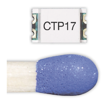
Nowadays, it is exceptional when an electronic part distributor gets also involved in component development. However, Endrich Bauelemente GmbH has engaged in it shoulder to shoulder with an excellent manufacturer (CT Micro) not yet widely known. The developer society shows great expectation for stepping forward in the world of optocouplers despite of the silence in recent decades. The target was to develop the thinnest device ever made and it has been successfully achieved using the CT MICRO DoubleMolded CoPlanar( DMC™) technology. The technical parameters have been defined by Phoenyx Contact, a client of Endrich being a market leader in its own field. In addition to the small size the extremely low profile was the most important requirement, 25% lower than the 2 mm high MiniFlat (SOP) packaging and 60% lower than the most common 4PDIP (DIL) packaging. CTP17 has been warmly welcomed by the visitors of the Electronica exhibition inMunich.
About the company CTMicro
CT Micro International Corporation is Customer oriented & Technology driven company which has been established to incorporate cutting-edge technical content into their products meeting the most serious requirements of market. The founders and leaders of the company are all experts having decades of experience in development, marketing and sales in the field of optoelectronic and MOSFET technologies. Since the technical leadership and the general management have dealt with infra-red components since more than 1 5 years, they can response to market needs implementing new products quickly using minimal effort. The target market is consumer electronics, white goods and industrial equipments. Knowing that quality products need quality components, CT Micro has established world class quality management during design and manufacturing.
The world thinnest transistor output optocoupler
It is a real challenge to create the “thinnest” among the optocouplers since the bigger the part is, the more space it can provide for physical insulation between the input and output to safely separate them even in case of higher potential difference.

The currently available thinnest components may not meet special customer requirements targeting solutions walking on the edge the current technology. CT Micro can provide such components. This new DFN packaging is 25% lower than the standard 2 mm high Mini-Flat (SOP) packaging and 60% lower than the most usual 4PDIP (DIL) packaging. It could be finally developed using the CT MICRO Double-Molded Co-Planar (DMC™) technology. This Ultra-Flat packaging (picture 1 ) makes it possible to develop the thinnest end product meeting the recent space saving requirements of the market. When the IR LED and the phototransistor are side-by-side inside the optocoupler, the structure is called co-planar. The optical link is ensured by some kind of reflective material inside the package. When the LED and the phototransistor are facing each other, we talk about “Over-Under” structure. The advantage of the first solution is the fixed insulation length resulting higher dielectric strength, and also the common mode noise suppression is better due to that no capacitive charge will develop between input and output opposed to the “over-under” structure. However, the “over-under” structure ensures more exactly adjusted current transfer rate (CTR). Additional advantage of the co-planar structure is that the LED and the phototransistor are located on the same lead frame, eliminating the need of positioning the input and output lead frames.
The engineers of CT-Micro have succeeded to unify the advantages of the co-planar and the over-under structures. The transmitter and the receiver is located on a single miniature PCB providing co-planar layout. The 2.5kVRMS insulation strength can be maintained by having more physical distance than 0.4 mm even if mechanical bending force is applied against the lead frame.

The translucent and reflective internal materials have equal thermal expansion rates ensuring preferable mechanical parameters. The first phase of injection molding carries the translucent material over the optoelectronic parts and the second builds up the reflective filling and the housing. The design on picture 2, makes it possible to create 2 and 4 channel devices. Parts with even higher insulation strength or saving more space can be offered in the future developing the carrying material even further. Concerning the optical behaviors, let us discuss the meaning ofCTR first.
The current transfer ratio (CTR) of an optocoupler is a notion similar to the DC current gain of transistors (hFE) and defined as a ratio of the output current (IC) to the input current (If).
CTR(%)=(IC/If) x 100
The CTR is as important attribute of an optocoupler as the insulation strength, and it is dependent on following factors:
- The driving current of the IR LED (IF)
- The ambient temperature
- The ware out of the optocoupler
Special attention must be paid to CTR during the design phase since not adequate tolerance may result insufficient output level resulting malfunctioned operation.

Picture 3 shows the dependence of CTR on the input current in case of an average optocoupler. It shows decreases of CTR on low current (If=1mA) and high current (If=20mA) input levels, and it is critical on the low level side. It is essential to set appropriate If to avoid malfunction due to small level of Ic.
CT Micro guarantees the CTR value to be between 100%-300% in case of If=1mA/ Vce=5V to support low driving current, flexible design and efficiency.
While the radiant intensity of the IR LED is reduced, the gain of the transistor is raised by higher ambient temperature; the dependency of CTR of the optocoupler is resultant of those factors and shown on picture 4:

Having an extended operational temperature range of -55°C to 1 25°C, this optocoupler satisfies the toughest challenges to meet requirements of industrial environment.

Apart from the RoHS (1 00% lead free) and REACH compliance, halogen free version is also available and obtaining UL and VDE certificates is already in progress.
| Share on Facebook | Share on LinkedIn |
References
This article has been published on the following locations:
| # | Media | Link |
|---|---|---|
| 1 | Elektronet 2017/1 | Elektronet : elektronikai informatikai szakfolyóirat, 2017. (26. évf.) 1. sz. 20-22. old. |
| 2 | Elektronet online | A világ legkisebb tranzisztoros kimenetű optocsatolója |
| 3 | Hungarian version | A világ legvékonyabb tranzisztoros kimenetű optocsatolója |
| 4 | TechStory M2M | A világ legkisebb tranzisztoros kimenetű optocsatolója |
| 5 | Jövő Gyára 2017/2 | 2017. 2.sz. 45-46.old. |
| 6 | PC & Industrie 2017/9 | 2017. 9.sz. 155-157.old. |