


Zoltán Kiss- Area Sales Manager - East Europe - Endrich GmbH.
Chip antennas for navigation applications
8 March 2013

Summary :
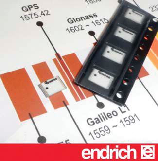
The satellite navigation is a system of satellites providing autonomous global geo-spatial positioning (longitude, latitude and altitude data) by emitting radio signals for electronic receivers located on the Earth, sea or air. Lately there are several systems with global coverage, the NAVSTAR Global Positioning System (GPS), the Russian GLONASS system and some of the systems are in development process, like the Chinese COMPASS, and the European Unions’s GALILEO system. Huge number of receiver devices are in use or in design phase, where the special antennas have key role in smooth operation.
Global coverage of these systems is generally achieved by using 20-30 medium Earth orbit (MEO) satellites distributed between several orbital planes from 2,000km to 35,786 kms of altitude. NAVSTAR GPS use the altitude of 20,200 km where the orbital period is 12 hrs, GLONASS satellites in Medium Earth Orbit have the altitude of 19,200 kms and Galileo ‘s located in altitude of 23,322 kms. GPS system uses frequencies of 1.57542 GHz (L1 signal) and 1.2276 GHz (L2 signal). GLONASS uses 1.602/1.246 GHz. Satellites broadcast signals, which contain their orbital data for calculating the position of the satellite as well as the exact time information the signal has been transmitted. All satellites of the constellation have synchronized time settings. Receivers decode the message and fetch out the time of broadcast, compare with the time of reception measured by an internal clock, in fact measuring signal time-to-fly to determine distance of the satellite from the receiver. Several measurements to different satellites provide enough data to use an enhanced trilateration process to calculate exact position and speed of the receiver. A critical part of the design of GPS receiver application is the antenna, the board and the signal path design - from the antenna to the module RF-input - has a big impact on system performance. As a general rule, when the antenna is located nearby to the module , within cca 15 cm, a passive antenna could be used, beyond this distance an active one should be used to cover the cable losses and achieve a good signal-to-noise ratio. The best selection of the antenna is based on the ideal mix of size, gain, bandwidth, noise and cost. Of course the external active antennas provide the best performance under low signal circumstances, but their size, power requirements and connection requirements make them expensive in certain cases. Ceramic passive patch antenna could be a low-cost choice providing omni-directional and sensitive solution, and because of small physical size it is possible to mount it on the same PCB as the module is located on. To maximize the performance the largest possible round plane under the antenna should be used. GPS receivers are becoming common not only for vehicle navigation systems, where normally space considerations are less important, but also used by default in almost all new cellular phones, tablets and other compact electronic devices. In these designs power consumption and physical size are key factors and subject to minimization. The optimization of space could be done by combining functionalities (e.g. WiFi / GPS) and using chip antennas designed onto the PCB.
Inpaq has developed new miniature ceramic antenna solutions (new coupling chip antenna generation) ACM4-5036-A1-CC-S and ACM0-3216-A1-CC-S. Both they are high efficiency miniature SMD edge mounted ceramic antennas with small footprint. Additionally this type of ceramic chip antenna uses the main PCB as its ground plane, thereby increasing antenna efficiency and allowing higher miniaturization. The ACM4 antenna for 1575MHz~1606 MHz band has an efficiency of 40-85% (depending on GND Size), which is at least three times the efficiency of traditional chip antennas. At a size of only 5.2*3.7*0.7mm (ACM4) and 3.2*1.6*0.5mm (ACM0) respectively, these devices are truly best-in-class antennas market in terms of efficiency and combination.
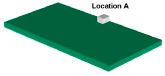
The ACM series works best when placed in the center of the side of the board, equal distance to the corner of PCB. However the antenna performance increases when the PCB size is enlarged, additionally the antenna still performs better than traditional linear polarized chip antennas even when placed nearby corners as substitute. The antenna is a modified dipole and requires no GND plane under component. Generally a passive antenna is a LC resonate circuit, the frequency notch influences the inductance whereas the chip influences the capacitance. The current travels at the surface of the PCB. The primary function of the notch size and component capacitance is setting center frequency and the PCB length determines the efficiency.
The antenna could be easily tuned to work for different PCB sizes by simply changing the value of the matching circuit. In summary, the chip antenna benefits are:
- Takes most advantage of the available ground plane for high efficiency, small footprint
- Peak efficiency 83% (Test board size on 80mm x 40mm)
- Peak Gain GPS/GLONASS to 3.2 dBi
- Substrate material is not critical to antenna performance. Less process variation
- Fully automated manufacturing process
- Chip Size 5.2mm x 3.7 mm x 0,7mm / 3.2 x 1.6 x 0.5mm
- Smallest keep out area
- Matching circuit requires small PCB area
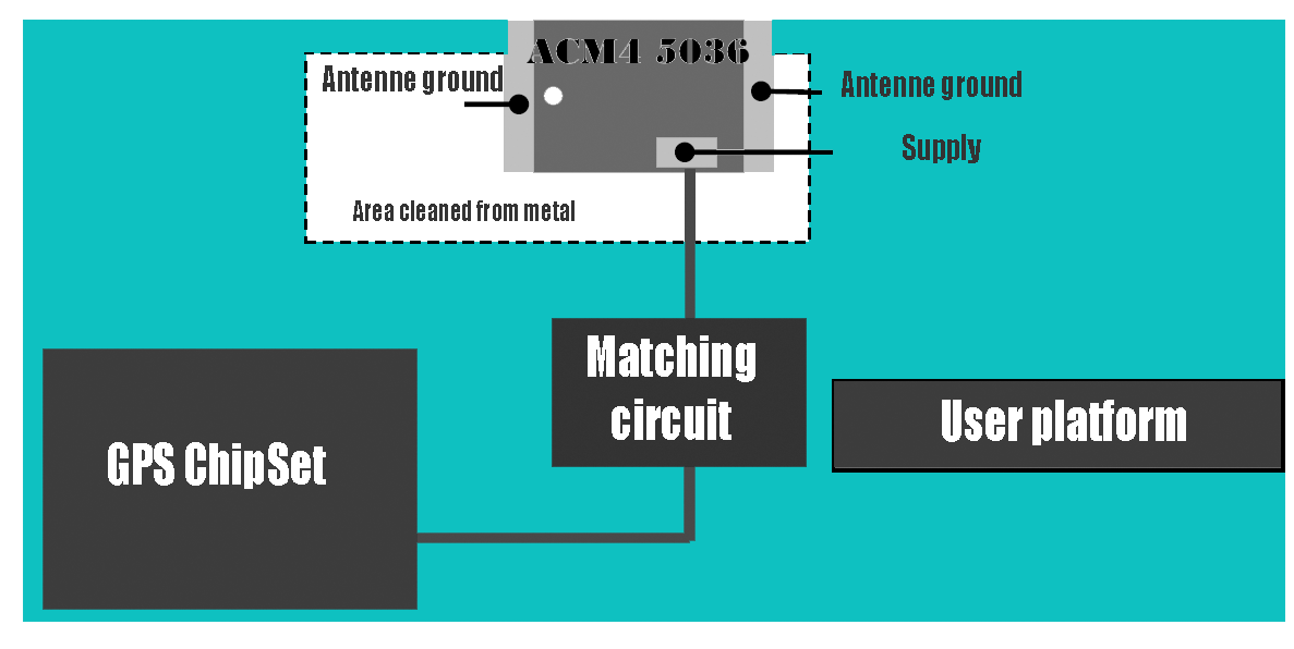
To achieve good antenna performance, the clearance area is necessary and all metallization should be removed from all PCB layers. To reduce return loss and shift the band to meet GPS application, there must be a PI-matching circuit used. For mobile phone applications, because most of the key components are arranged along the long side of the PCB, there is no space to place the antenna. Better to move it to the top edge of PCB. As the impedance of PCB at the top edge is smaller than in long side edge, a narrower bandwidth and lower performance will be resulted than in long side of PCB. But we still get a workable performance by arranging antenna and components in a reasonable position. In applications, where PCB size is smaller because of presence of other spare parts, like batteries, additional tricks could be done. The smaller the PCB is, the worst antenna performance will be resulted. According to the characteristic of the antenna, the radiation efficiency depends on the size of the metal layer. By extending the metal layer from PCB to panel using copper foil, the radiation plane can be extended, the PCB size becomes a minor factor of antenna performance.
| Share on Facebook | Share on LinkedIn |
References
This article has been published on the following locations:
| # | Media | Link |
|---|---|---|
| 1 | Elektronet 2013/2 | Elektronet : elektronikai informatikai szakfolyóirat, 2013. (22. évf.) 2. sz. 34-35. old. |
| 2 | Elektronet online | Chip-antennák navigációs alkalmazásokhoz (GPS/GLONASS) |
| 3 | Hungarian version | Chip antennák navigációs alkalmazásokhoz (GPS/GLONASS) |