Zoltán Kiss- Area Sales Manager - East Europe - Endrich GmbH.
DC-DC switching power supply regulators from new japan radio corporation
6 December 2013
![]()
Summary :
DC/DC converters are essential elements of today’s battery driven consumer electronics devices, which often contain subsystems with own level of required supply voltage. Mainly the lack of the available space forces designers not to use different batteries but use voltage converters to produce various voltages available, sometimes even higher than the battery voltage, and often provide regulated output, which is important as the battery voltage decreases by loosing the stored power. DC-DC converters, which convert the input voltage to a lower level are called step-down or buck converters, the ones producing higher voltage than the battery voltage are called step up or boost converters.
General overview of voltage regulation
To produce different voltage levels out of the battery voltage could be done on several ways, like using resistor based voltage dividers, or linear regulators, but these solutions can only provide lower level of voltages and the efficiency is low, as - if the voltage drop is high and the current is large- , the excess power will be lost by dissipating remarkable heat. Better to use today switching mode DC/DC converters, which temporarily storing energy in magnetic or electric storage components and releasing this energy to result different voltage level on the output. The efficiency will be remarkable higher resulting better battery lifetime at the end.
Step Down / Buck converters
Those switching more DC/DC converters, that are characterized by lower Vout than Vin are generally called step down or buck converters. Their working principle is based on the ideal circuit shown in figure 1.
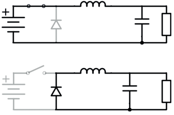
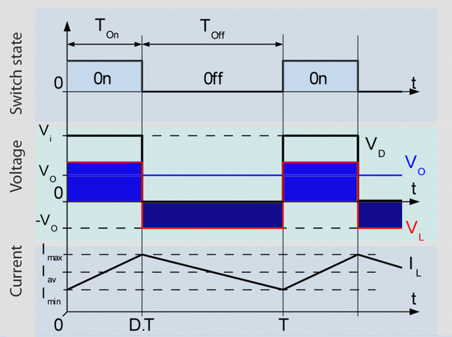
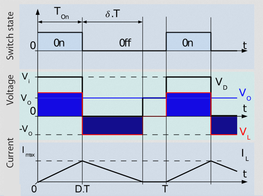
The switch on the circuit represents the element that is used for connecting and disconnecting the circuit and the battery, which is in reality a MOSFET or an IGBT component. The inductor is used for storing the energy, by building up its magnetic field right after the battery is connected to the circuit. During charging, the inductor would produce a voltage drop that is reducing the voltage of the load. If the switch opens before the charging is complete, the output voltage remains always less than the battery voltage. At this moment the flyback diode switches on, and provides a closed circuit, which could then discharge the energy stored in the magnetic field. As long as the switch off period is shorter than the discharge time of the inductor, the voltage of the load is always higher than zero, as the inductor pumps energy and supports current flowing through the load. The average voltage on the output is always lower than the input supply voltage. The parallel capacitor is placed for smoothing the ripple voltage resulted by fluctuation of voltage in each cycles of switching. Operating mode of the DC/DC step down converter is continuous mode, when the current of the inductor cannot decrease to zero. If the energy stored in the inductor is not large enough to supply the current in the whole switch off state of the cycle, the current will be zero for the part of the cycle. This operation mode is called discontinuous mode. The figures show the differences:
Synchronous switching
There is an enhanced version of buck regulators, which is inherited from the conventional step down converter circuitry. In this type the flyback diode is replaced by a complementary-out driver operated second switching element (lower switch). As the switch element (MOSFET/IGBT) has definitely lower Rdson value, the power loss resulted by the voltage drop of the flyback diode used in the conventional solution will be reduced. In both cases the power loss is dependent on the duty cycle. The other advantage of this solution is that the converter is bi-directional. This solution is however a compromise between higher cost (more expensive elements) a better performance.
Control modes
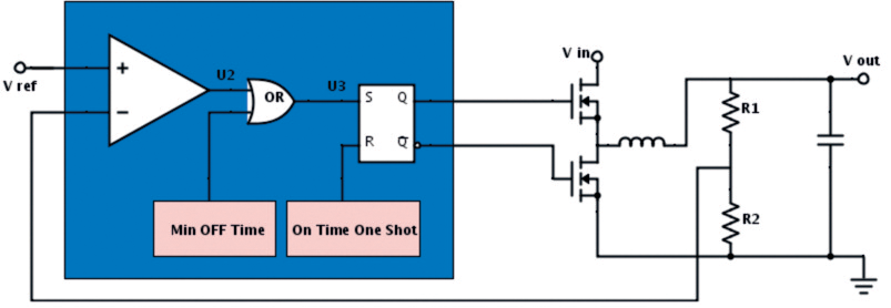
Most common control mode of the switching more voltage regulators is the fixed frequency PWM (Pulse With Modulation) control, where a PWM control circuit provides the complementary switching. The other well known control mode is the hysteretic voltage control. In this solution no oscillator is needed, therefore no issues with the frequency compensation. The system is using a comparator, where upper and lower threshold values are set up. The voltage ripple on the output connected as a kind of feedback to the comparator, and when the ripple voltage exceeds the high reference value, the high side switch turns off, the low side switch turns on, the output voltage falls down, therefore ripple will be also reducing. Constant on time (COT) control regulators need no oscillator and also use the output ripple voltage to initiate switching ON, but this case the high side switch stays switched ON for a fixed duration. Advantage of such a construction is the higher efficiency on light load as well as the fast transient response. However for these solutions the out put capacitor should have a high ESR in order to produce ripple voltage high enough, which means noise sensitivity on output.
Power converter self protection
In order to improve the power converter reliability the producers apply several kind of self protections. Moreover conventional non recoverable protection modes (fuses, circuit breakers) and resettable protection (PolySwitches), DC/DC converters are equipped with self recoverable protection features. Cycle-by-Cycle current limiting protection detects the overload condition and limits the duty cycle. In this case the high side switch is ON just for a short time, therefore the buck diode is carrying the load current for long time resulting thermal management problem. Unless the diode and the heatsink is oversized this condition delivers to a lifetime issue. The hiccup mode current-limiting scheme can overcome the disadvantages. Once an overload situation is detected the converter is switched off and forced into sleep mode for a defined time. A the end of he sleep time, a restart attempt is made and if the overload condition persists, the process is repeated. In constant overload situation the converter experiences a series of bursts followed by sleep time, hence the name ‘hiccup’ mode.
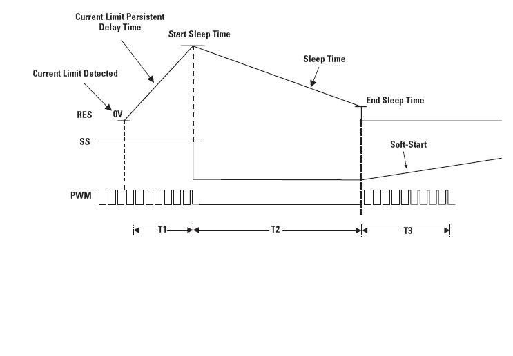
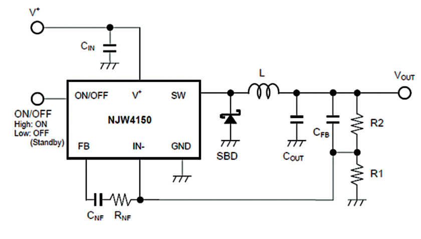
The sleep time reduces the average current and allows the converter to cool down New Japan Radio’s NJW4150 is a switching regulator IC for buck converter with 34V, 450mA MOSFET. It corresponds to high frequency oscillating, wide input voltage and Low ESR Output Capacitor (MLCC). Therefore, the NJW4150 can realize downsizing of applications with a few external parts, makes it suitable for power supply circuit of Car Accessory, Office Automation Equipment and Industrial Instruments.
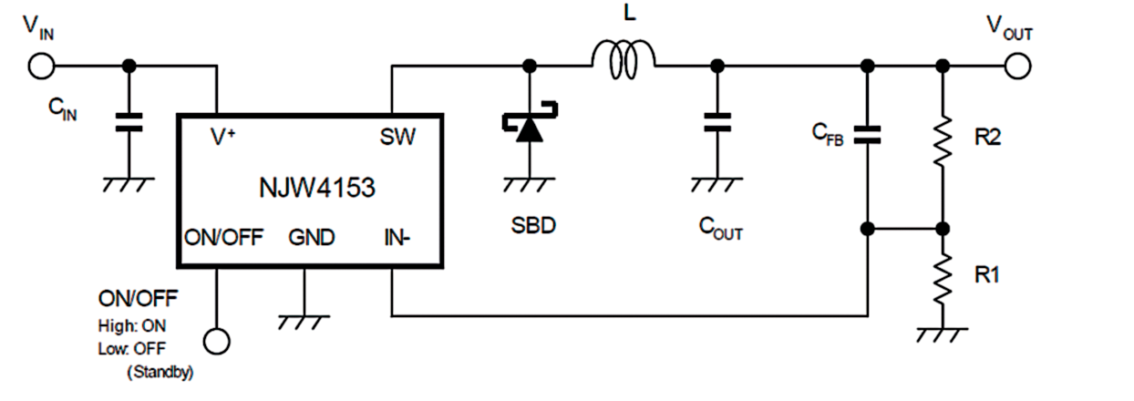
An other solution is the NJW4153 buck converter with 40V/1A MOSFET within wide input range from 4.6V to 40V, that adopts current mode control with just a few additional spare parts around. It is suitable for power supply circuit of Micro Processor, DSP, that need fast transient response.
Step Up / Boost converters
Those switching more DC/DC converters, that are characterized by higher output voltage than supply voltage are called step up or boost converters. The ideal circuit diagram presents the working principle :
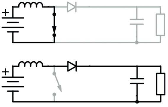
When the switch is “on”, the inductor starts to charge, while load voltage is zero. Once the switch is open the energy stored in the magnetic field is starting to support current flowing through the load, and the two sources in series are causing higher voltage to charge the capacitor through the diode. When the switch is again off, the diode prevents the capacitor to discharge. If the switching is fast enough, the inductor will not discharge completely before the next charging cycle, therefore the output voltage is always higher than the voltage of the power source alone.
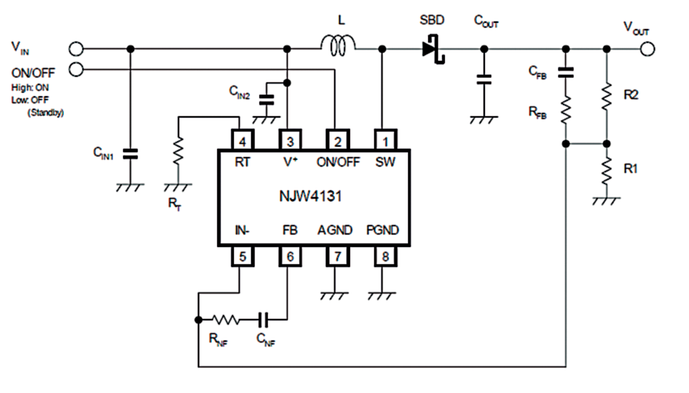
One of the popular boost converter solution is the New Japan Radio NJW4131 with 40V/1.4A or 40V/1A MOSFET. It corresponds to high oscillating frequency, and Low ESR Output Capacitor (MLCC) within wide input range from 4.0V to 35V. Therefore, the NJW4131 can realize downsizing of an application with a few external parts. Also, it has a soft start function, an over current protection and a thermal shutdown circuit. It is suitable for power supply to a Car Accessory, Office Automation equipment, Industrial Instrument, LED driving. The sample circuit diagram is shown on the figure.
Please consult the author concerning several DC/DC converter solutions for your own design.
| Share on Facebook | Share on LinkedIn |
References
This article has been published on the following locations:
| # | Media | Link |
|---|---|---|
| 1 | Elektronet 2013/8 | Elektronet : elektronikai informatikai szakfolyóirat, 2013. (22. évf.) 8. sz. 24-25. old. |
| 2 | Elektronet online | DC/DC kapcsolóüzemű feszültségátalakítók |
| 3 | Hungarian version | DC-DC kapcsolóüzemű feszültség átalakítók - New Japan Radio Corp. |
| 4 | TechStory M2M | DC/DC kapcsolóüzemű feszültségátalakítók működése |
| 5 | Jövő Gyára 2018/2 | 2018. 2.sz. 33-34.o. |
| 6 | Magyar Elektronika online | DC/DC kapcsolóüzemű feszültségátalakítók a New Japan Radio Corporation-től |
| 6 | Magyar Elektronika 2019/4 | 2019. 4.sz. 25-26.o. |


